
Universal Wirelist Conversion Program
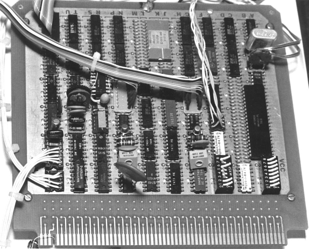
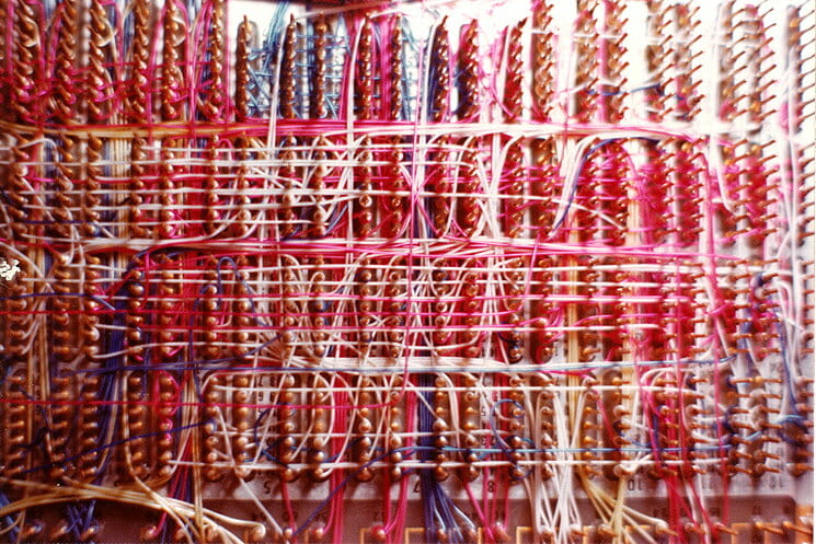
For many years I had a simple rule: all projects, whether hobby or consulting, had to have at least one associated magazine article. I didn’t always manage to accomplish this, but did so here; back in 1978, I landed an industrial control gig for Robinson-Nugent, and had to build a machine that would do insertion/withdrawal force tests on the fly as one of their assembly machines produced Quick-Connect pin sockets. If a given one was out of spec, I had to whack it at the right point during its path through the machine to break it off a carrier strip and launch it into a reject bin… and in the process, maintain a statistical analysis of quality. I published the solenoid-driver circuit in Machine Design, and an esoteric BASIC program to help convert the wire list of the logic board to something that played nice with a universal pin layout. I always wondered if anyone else ever found this at all useful, but it was a nice trade-journal article to have in the portfolio. The photo above shows the board.

by Steven K. Roberts, Cybertronics
Electronic Packaging and Production
September, 1980
Computer program maps a standard wirelist for the pins of a universal wire wrapping panel.
When one sets about to prototype a digital circuit, there are a number of choices to be made which can govern both the quality of the final product and its ease of execution. One such situation is the construction of a board containing a variety of “odd-sized” ICs, whether as a production prototype or as a one-of-a-kind custom system. For a number of reasons, the use of a printed circuit board at this level is generally undesirable, so wire wrapping is a reasonable choice of assembly technique. But with chips of various sizes populating the board, it can be difficult to adapt to an off-the-shelf wrap panel with dedicated IC patterns.
There’s an alternative, of course: the universal wire wrapping panel. Basically an undifferentiated matrix of pinsockets arranged in rows located on 0.3 in. centers, this type of panel allows most standard IC packages to be inserted at arbitrary locations without the layout restrictions of dedicated panels.
These universal panels have been in existence for some time, but have classically suffered some lack of popularity: wiring them is an ordeal. After a few hours hunched over a blurred sea of Kynar with a sweaty wrap gun in hand, even a veteran wirewrapper tends to experience an unpleasantly high probability of error. The problem, essentially, is that the lack of representative IC pin numbering, compounded by the lack of visible boundaries between chips, makes accurate placement of wires considerably more difficult than is the case on “standard” cards. The need to visually resolve arbitrary pins amidst hundreds of identical neighbors while correlating X-Y pin designations with a schematic or wirelist has been responsible for more than a few headaches.
It was a recent project involving one such card (Fig. 1) that spawned the technique described here: the use of a small computer to map a standard wirelist for the circuit onto the X-Y pin designations of the wire wrapping panel. The resulting wirelist can be used by an assembly technician to build the board, without further attention to the placement of individual chips or their relationships with the pin numbering of the universal card. This dramatically simplifies and speeds the task, while reducing the probability of wiring errors.
The computer program, written in the BASIC language, makes no restrictions on the size or configuration of the universal panel involved; it merely calculates the new “row” and “level” numbers for each IC pin specified by the user. It is thus possible to offer this program as a widely applicable engineering tool.

Use of the program
The universal wirelist conversion program, shown in its entirety in the accompanying listing (Fig. 2), should run with only minor modifications on any computer hosting a BASIC interpreter. The fact that any modification at all may be required is the result of an unfortunate situation: unlike FORTRAN, COBOL, and other industry standard computer languages, BASIC—the most common of all—was never defined in “standard” form by ANSI or anyone else. There thus exist in the marketplace perhaps a dozen slightly different dialects of BASIC, each hailed as the best by the manufacturer of its host computer. Fortunately, however, the language is so widespread by this time that this doesn’t seem to be a crippling problem—just occasionally annoying for anyone having to change a few statements to make a published program run on his own machine. To simplify this task for those interested in using this program, we will describe the function of each statement in detail later in this article.
But first, a description of the program’s use is in order. Take a look at lines 1100-1300 of the listing.
These DATA statements are used to tailor the program to the specific task at hand: they comprise a complete definition of the desired chip (IC, component) layout and package sizes. Each DATA statement provides the program with all the information it needs about one chip, and there can be any number of them up to 100 (this is rather arbitrary, and can be trivially increased by changing the variable in line 240 to five times the maximum number of devices you anticipate using).
Setting up the DATA statements for a project is simple—for each IC, the following five pieces of information are needed:
- Reference number from circuit diagram
- Number of pins on IC package
- Width (in multiples of 0.3 in.)
- Pin 1’s row
- Pin 1’s level
Item 1 identifies the device and is the means by which interconnections will be specified to the program (such as Chip 7, Pin 2). Items 2 and 3 define the physical size of the IC, and items 4 and 5 define its location on the panel.
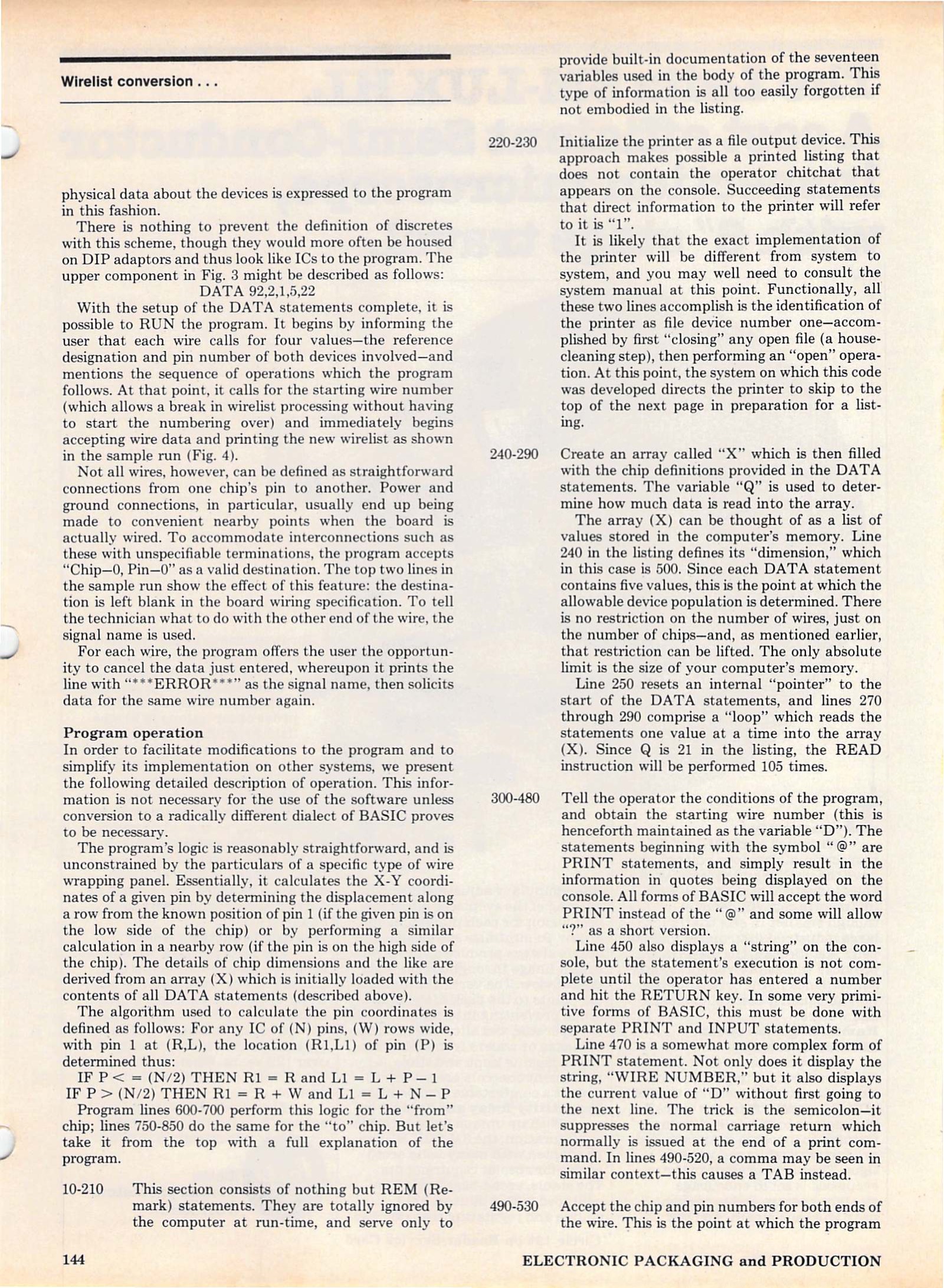
Let’s consider some examples. In Fig. 3, a section of a universal wrap panel is sketched which contains three chips (one each of 6-pin, 14-pin, and 24-pin) and two discrete components. For the 14-pin chip, the data statement would read,
DATA 21,14,1,5,23
while the 24-pin chip would produce the following:
DATA 34,24,2,7,22
It should be clear from examination that all pertinent physical data about the devices is expressed to the program in this fashion.
There is nothing to prevent the definition of discretes with this scheme, though they would more often be housed on DIP adaptors and thus look like ICs to the program. The upper component in Fig. 3 might be described as follows:
DATA 92,2,1,5,22
With the setup of the DATA statements complete, it is possible to RUN the program. It begins by informing the user that each wire calls for four values—the reference designation and pin number of both devices involved—and mentions the sequence of operations which the program follows. At that point, it calls for the starting wire number (which allows a break in wirelist processing without having to start the numbering over) and immediately begins accepting wire data and printing the new wirelist as shown in the sample run (Fig. 4).
Not all wires, however, can be defined as straightforward connections from one chip’s pin to another. Power and ground connections, in particular, usually end up being made to convenient nearby points when the board is actually wired. To accommodate interconnections such as these with unspecifiable terminations, the program accepts “Chip—0, Pin—0” as a valid destination. The top two lines in the sample run show the effect of this feature: the destination is left blank in the board wiring specification. To tell the technician what to do with the other end of the wire, the signal name is used.
For each wire, the program offers the user the opportunity to cancel the data just entered, whereupon it prints the line with “ERROR” as the signal name, then solicits data for the same wire number again.
Program operation
In order to facilitate modifications to the program and to simplify its implementation on other systems, we present the following detailed description of operation. This information is not necessary for the use of the software unless conversion to a radically different dialect of BASIC proves to be necessary.
The program’s logic is reasonably straightforward, and is unconstrained by the particulars of a specific type of wire wrapping panel. Essentially, it calculates the X-Y coordinates of a given pin by determining the displacement along a row from the known position of pin 1 (if the given pin is on the low side of the chip) or by performing a similar calculation in a nearby row (if the pin is on the high side of the chip). The details of chip dimensions and the like are derived from an array (X) which is initially loaded with the contents of all DATA statements (described above).
The algorithm used to calculate the pin coordinates is defined as follows: For any IC of (N) pins, (W) rows wide, with pin 1 at (R,L), the location (Rl.Ll) of pin (P) is determined thus:
IF P < = (N/2) THEN R1 = R and L1 = L + P – 1
IF P > (N/2) THEN R1 = R + W and L1 = L + N – P
Program lines 600-700 perform this logic for the “from” chip; lines 750-850 do the same for the “to” chip. But let’s take it from the top with a full explanation of the program.
10-210 This section consists of nothing but REM (Re mark) statements. They are totally ignored by the computer at run-time, and serve only to provide built-in documentation of the seventeen variables used in the body of the program. This type of information is all too easily forgotten if not embodied in the listing.
220-230 Initialize the printer as a file output device. This approach makes possible a printed listing that does not contain the operator chitchat that appears on the console. Succeeding statements that direct information to the printer will refer to it is “1”.
It is likely that the exact implementation of the printer will be different from system to system, and you may well need to consult the system manual at this point. Functionally, all these two lines accomplish is the identification of the printer as file device number one—accomplished by first “closing” any open file (a house-cleaning step), then performing an “open” operation. At this point, the system on which this code was developed directs the printer to skip to the top of the next page in preparation for a listing.
240-290 Create an array called “X” which is then filled with the chip definitions provided in the DATA statements. The variable “Q” is used to determine how much data is read into the array.
The array (X) can be thought of as a list of values stored in the computer’s memory. Line 240 in the listing defines its “dimension,” which in this case is 500. Since each DATA statement contains five values, this is the point at which the allowable device population is determined. There is no restriction on the number of wires, just on the number of chips—and, as mentioned earlier, that restriction can be lifted. The only absolute limit is the size of your computer’s memory.
Line 250 resets an internal “pointer” to the start of the DATA statements, and lines 270 through 290 comprise a “loop” which reads the statements one value at a time into the array (X). Since Q is 21 in the listing, the READ instruction will be performed 105 times.
300-480 Tell the operator the conditions of the program, and obtain the starting wire number (this is henceforth maintained as the variable “D”). The statements beginning with the symbol “@” are PRINT statements, and simply result in the information in quotes being displayed on the console. All forms of BASIC will accept the word PRINT instead of the “@” and some will allow “?” as a short version.
Line 450 also displays a “string” on the con sole, but the statement’s execution is not complete until the operator has entered a number and hit the RETURN key. In some very primitive forms of BASIC, this must be done with separate PRINT and INPUT statements.
Line 470 is a somewhat more complex form of PRINT statement. Not only does it display the string, “WIRE NUMBER,” but it also displays the current value of “D” without first going to the next line. The trick is the semicolon—it suppresses the normal carriage return which normally is issued at the end of a print command. In lines 490-520, a comma may be seen in similar context—this causes a TAB instead.
490-530 Accept the chip and pin numbers for both ends of the wire. This is the point at which the program accepts from the operator the data which, along with the contents of the array, will be used to calculate the X-Y designations of the pins on the board. The values which the operator enters as cued become stored in the four variables, F, A, T, and B. The lone ” ” in line 530, as well as those in lines 320, 330, 390, 440, 460, and 480, simply cause a carriage return on the console, skipping a line to provide an easy-to-read display.
540-560 Accept the signal name and store it in the string “N$”. This is a different form of the INPUT statement we discussed earlier: instead of a numeric value, it accepts any arbitrary string of text terminated by a carriage return, then stores it in memory under a specified name. The DIM statement in line 540 defines the maximum length, and was arbitrarily placed at the unnecessarily high value of 100.
570-590 Begin printing the wirelist entry with the current wire number and the word, “Board:” (see Fig. 4).
Throughout the program, information to the printer is formatted by the PRINT USING commands, which result in even, right-justified columns of numbers on the page. This is another area in which there is some variation between dialects of BASIC, and experimentation is in order if it acts strange on your system.
600-700 Compute the row and level pin coordinates for the “from” chip by indexing into the array (X) with the chip number, obtaining the package specifications, and determining via the algorithm described earlier whether the pin number in question is on the low or high numbered side of the chip. By the time the computer arrives at line 710, the values Rl and Ll contain the actual location of the specified pin on the board.
710-730 Display the computed coordinates on the con sole and also print them on the wirelist. Note the combination of strings, numeric values, and tabs in the PRINT (“@”) statement in line 710.
740 Skip the computations for the other end of the wire if the “to chip/pin” was 0/0. This is the case, you may recall, where the destination is unspecifiable until wiring time, as in the case with Vcc and Gnd.
750-850 Compute the row and level pin coordinates for the “to” chip in exactly the same manner as the computations in lines 600-700 for the “from” chip.
This is an area in which some space could be saved, possibly, by creating a “subroutine” to perform these calculations. This would be implemented by separating the ten instructions, terminating them with a RETURN statement, and executing them with a GOSUB from either of the two places in the code where the operation is needed. This wasn’t done, however, because the added effort of passing parameters to and accepting data from the subroutine would have created more complexity than it would have eliminated. This is a common error in software design—eagerness to use subroutines everywhere possible can have unpleasantly convoluted results.
860-880 Display the destination coordinates on the console and also print them on the wirelist.
890-930 Print the input information on the wirelist so that there is a “hard-copy” reference to the original data and thus to the schematic. If this were not done, errors in entry would be exceedingly difficult to spot—after all, the intent here is the elimination of mistakes.
940-990 Solicit a “Y” or “N” response to the question, “OK?”, and print either the error message or the signal name accordingly (see wire 104 on the sample run in Fig. 4). If the wire was in error, “D” is reduced by 1 to keep the wire numbering scheme intact.
1000-1020 Skip three lines on the printer so wirelist falls within standard line markings on fanfold paper. This is optional, but it is nice to have ample room for penciled-in notes and changes (they are inevitable).
1030 Increment the wire number.
1040-1070 Clear the screen and return to line 470 to start on another wire. Most CRT terminals have “clear screen” commands, but the program makes no assumptions—it just does 23 carriage returns. If your console is a hard-copy terminal (such as a teletype), you would obviously want to get rid of Lines 1040-1060 so you could use the same roll of paper for more than a couple of hours.
1080-1090 Print blanks to skip destination information on wirelist. This statement is executed only when the test at line 740 detects a “0,0” destination.
1100-1300 These are the DATA statements denning one particular configuration of 21 chips, as discussed earlier.

Implementation
The program makes no esoteric demands on the configuration of its host system, so there should be no problem with implementation on any of a variety of computers. Small “hobby” systems, provided they have a halfway decent BASIC, enough memory, and some form of hard-copy output, will do the job as easily as large time-share networks.
The use of this program has reduced errors and eliminated many of the headaches which are classically involved in the prototyping of digital circuits (such as the one in Fig. 1) on universal wire wrapped cards. Since the person doing the construction need not make the continual translation between the pin designations used in the circuit diagram and the coordinates on the board, the process is significantly faster as well.
Steven K. Roberts is a self-employed writer and consultant. The bulk of his experience in microprocessor system design and IC pack aging stems from his five-year presidency of Cybertronics, Inc., a custom engineering firm. He has written and published 30 articles on related subjects, published one book (Micromatics, Scelbi Publications), and is working on a second.

You must be logged in to post a comment.